

 受験生の方へ
 企業・研究者の方へ
 在校生の方へ
 市民の方へ
市民の方へ 卒業生の方へ
 学内教職員用
キラー欠陥を従来の10分の1に低減した 第3世代酸化ガリウム100 mmエピウエハーの開発に成功 ―100 A級酸化ガリウムパワーデバイスの実現が可能に―


株式会社ノベルクリスタルテクノロジー
国立大学法人佐賀大学
NEDO(国立研究開発法人新エネルギー・産業技術総合開発機構)
(The English version is below.)
NEDOの「戦略的省エネルギー技術革新プログラム」において「β-Ga2O3ショットキーバリアダイオードの製品化開発」に取り組む(株)ノベルクリスタルテクノロジーは、このたび佐賀大学と共同で第3世代酸化ガリウム100 mmエピウエハーを開発しました。本開発では、エピウエハー製造技術を改良し、酸化ガリウムパワーデバイスの大電流化を阻害していた耐圧特性を劣化させる欠陥(キラー欠陥)を従来の10分の1に低減させました。
本開発の成果により、電車や産業機器、電気自動車などの100 A級のパワーデバイスが求められる市場に酸化ガリウムパワーデバイスを広く展開することが可能となり、省エネルギー化とともにカーボンニュートラルの実現に向けた大きな前進が期待できます。
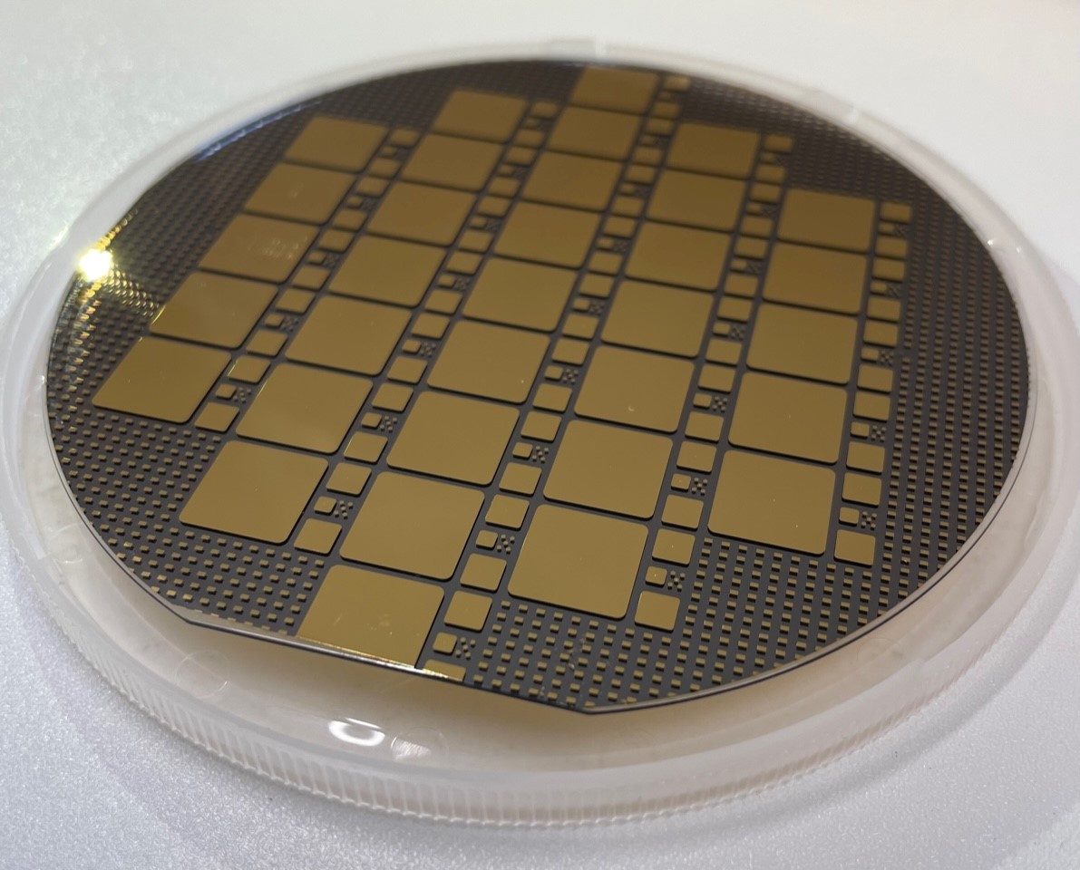
図1 第3世代β-Ga2O3 100 mmエピウエハーを用いて試作したショットキーバリアダイオード.
最大のチップサイズは10 mm×10 mm
1.概要
酸化ガリウム(β-Ga2O3)は、電力損失の小さいパワーデバイスを低コストで実現できる新材料として注目を集めています。パワーデバイスは家電や自動車、電車、産業用機器などあらゆる電気機器の中で、電圧や電流を制御するために使われています。従来のパワーデバイスはシリコンを使って作られてきましたが、電力制御の際の電力損失の発生が課題でした。その損失の低減のために、炭化ケイ素(SiC)や窒化ガリウム(GaN)を材料としたパワーデバイスの開発が進められていますが、β-Ga2O3を使うことで、さらに電力損失を小さくし、電気機器の消費電力を削減することができます。また、SiCやGaNより高速な製造手法を用いることができるため、低コスト化が期待できます。このため現在国内外において、β-Ga2O3パワーデバイスの早期実用化に向けた研究開発が進んでいます。
こうした中、株式会社ノベルクリスタルテクノロジーは国立大学法人佐賀大学と共同で、NEDO(国立研究開発法人新エネルギー・産業技術総合開発機構)の「戦略的省エネルギー技術革新プログラム」において、β-Ga2O3パワーデバイスの製品化を目指す「β-Ga2O3ショットキーバリアダイオードの製品化開発」に取り組んできました。今回、β-Ga2O3のエピウエハー※1製造技術を改良することにより、デバイスの耐圧特性を劣化させる欠陥(キラー欠陥※2)を従来の10分の1まで低減させた第3世代β-Ga2O3 100mmエピウエハーの開発に成功し、300A~500A級の大型酸化ガリウムショットキーバリアダイオード※3を試作しました(図1)。これを活用することで、電気自動車などの100A級のパワーデバイスが求められる広い市場へ、β-Ga2O3パワーデバイスの展開が可能となります。これにより、2030年代におけるその省エネルギー効果は原油換算で年間10万kL以上にもなり、省エネルギー化とともに2050年カーボンニュートラル実現に向けた大きな前進が期待されます。
2.今回の成果
(株)ノベルクリスタルテクノロジーではすでにβ-Ga2O3エピウエハーを100mmまでスケールアップしたエピ成膜装置を開発※4し、第2世代β-Ga2O3 100mmエピウエハーとして製造・販売を行ってきました。しかし、この100mmエピウエハーにはデバイスの耐圧特性を劣化させるキラー欠陥が10個/cm2程度存在するため、大型のデバイスを作ることができず、電流値は10A程度に制限されていました。この課題の解消を目指して、佐賀大学との共同研究により、キラー欠陥の原因が主にエピ成膜中に発生する特定の粉体であることを突き止めました。そして、エピ成膜条件を改良することにより、キラー欠陥を従来の10分の1以下の0.7個/cm2まで低減した第3世代β-Ga2O3 100mmエピウエハーを実現しました。
【1】膜厚およびドナー濃度の面内分布の検証
最初に、改良した条件で作製した第3世代β-Ga2O3 100mmエピウエハーの膜厚分布と、ドナー濃度※5の分布を調べました。結果を図2に示します。パワーデバイス用のエピウエハーには、キラー欠陥の密度だけでなく、膜厚およびドナー濃度の高い均一性が求められます。エピウエハー面内9点の膜厚分布とドナー濃度分布を測定したところ、それぞれ10μm±5%程度、1×1016cm-3±7%程度と非常に小さく、パワーデバイス用として問題ないうえ、第2世代エピウエハーのおよそ7分の1に改善していることがわかりました。
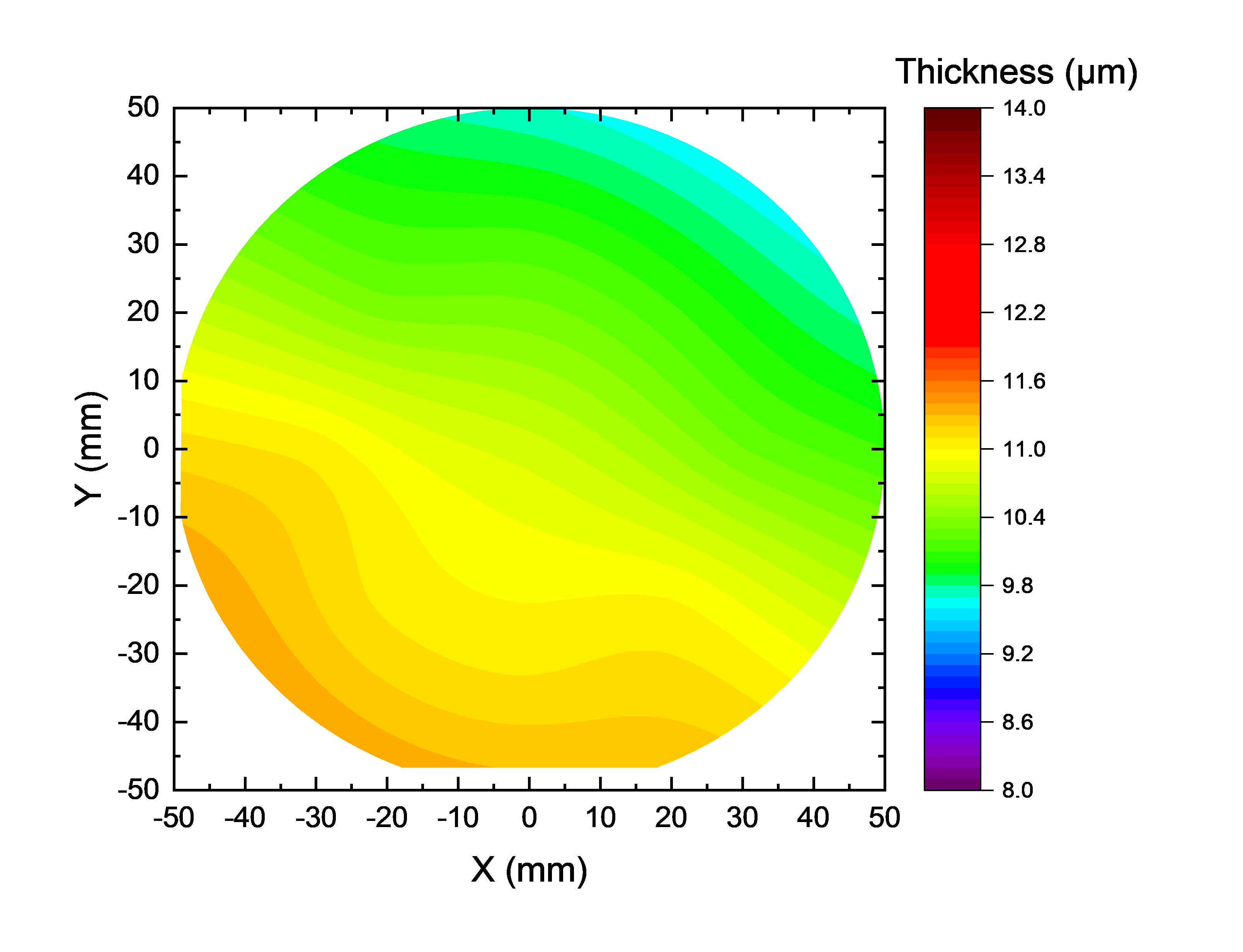
(a)膜厚分布 (b)ドナー濃度分布
図2 第3世代β-Ga2O3 100 mmエピウエハーの(a)膜厚分布と(b)ドナー濃度分布
【2】キラー欠陥密度の検証
つぎに本エピウエハー上にβ-Ga2O3ショットキーバリアダイオード(図1)を試作し、電気特性とキラー欠陥密度を評価しました。図1に示したウエハー表面の複数の電極パターンの中で、一番大きいものが今回の評価に用いた10 mm×10 mmのβ-Ga2O3ショットキーバリアダイオードです。これらのダイオードの電流‐電圧特性を示したものが図3です。図3(a)の順方向特性を見ると、電流は0.8 V程度から流れ始めて一定に上昇しており、正常な順方向特性が得られていることが分かります。最大電流値は50 Aとなっていますが、これは測定に用いた機器(プローバ)の制限によるもので、本デバイスは最大で300~500 A流すことが可能です。次に図3(b)の逆方向特性を見ると、200 V程度加えてもリーク電流は10-7 A程度に抑制することができています。今後、デバイスに電極終端構造※6を設けることで、600~1200 V程度の耐圧が得られると推定されます。
試作した10 mm×10 mmのβ-Ga2O3ショットキーバリアダイオードの逆方向特性歩留まりは51%であり、その値と今回実証に用いた電極サイズから、キラー欠陥密度は0.7個/cm2程度と推定されました。これは、100 A級のβ-Ga2O3パワーデバイスを、80%程度の歩留まりで製造可能なことを意味しています。
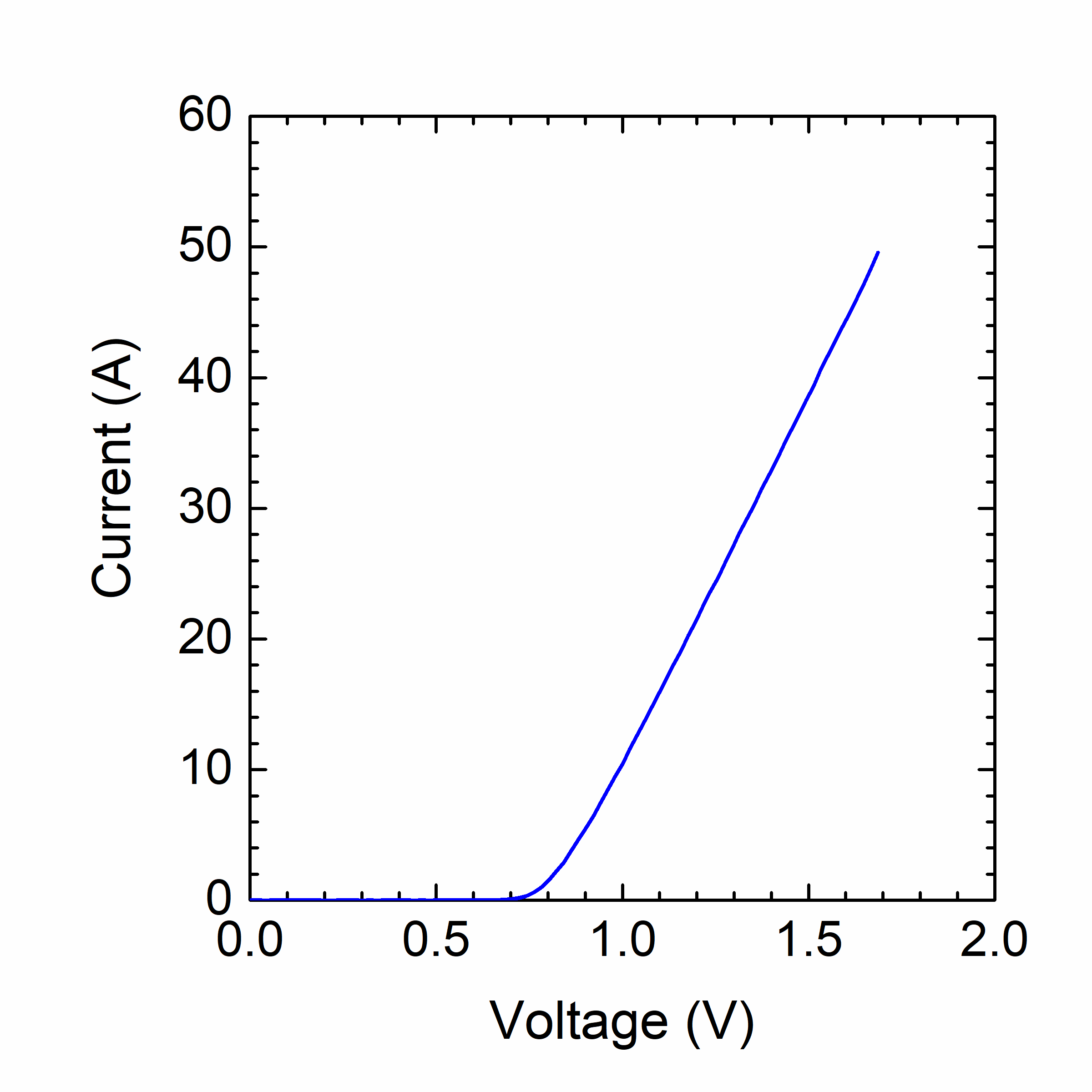
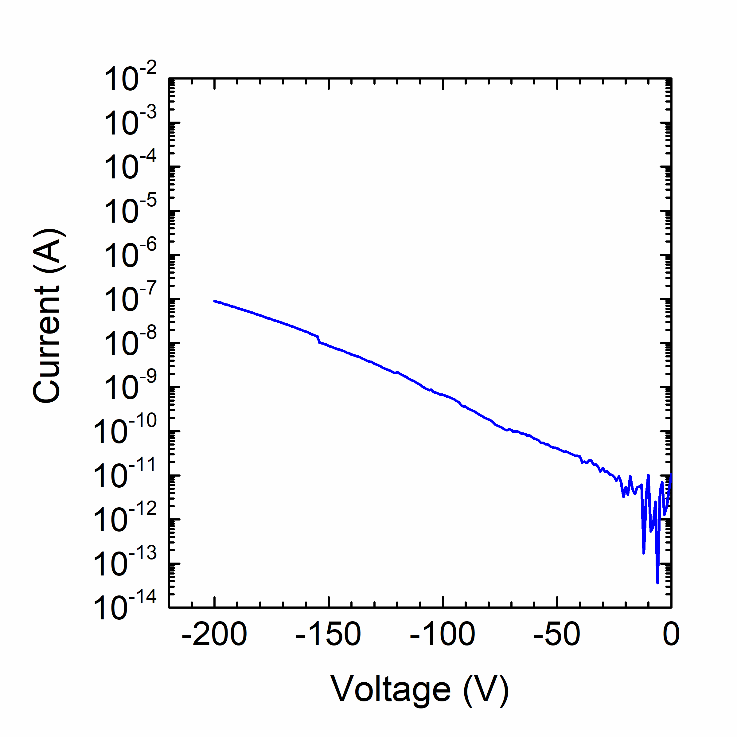
(a)順方向特性 (b)逆方向特性
図3 ショットキーバリアダイオードの(a)順方向と(b)逆方向の電流‐電圧特性
3.今後の予定
(株)ノベルクリスタルテクノロジーは新開発した第3世代β-Ga2O3100mmエピウエハーの製造ラインを構築し、早期に販売を開始します。今後、ドナー濃度および膜厚の指定範囲の拡大を進めるともに、キラー欠陥のさらなる低減と大口径化に取り組みます。また、NEDO事業において同社はすでに、トレンチ構造※7を導入した1200V耐圧の電力損失が小さいβ-Ga2O3ショットキーバリアダイオードの実証にも成功※8しており、今後、本開発製品を用いた1200V耐圧トレンチ型ショットキーバリアダイオードの量産技術の構築を進めていきます。
NEDOは本技術開発をはじめ、今後も経済成長と両立する持続可能な省エネルギーの実現を目指し、「省エネルギー技術戦略」で掲げるエネルギー・産業・民生(家庭・業務)・運輸部門などにおける重要技術を中心に、2030年には高い省エネ効果が見込まれる技術について、事業化までシームレスに技術開発を支援します。
【注釈】
※1 エピウエハー
単結晶基板上に結晶膜が形成されたウエハーをいいます。主に結晶膜に機能を持たせるため、結晶膜の品質が重要となります。
※2 キラー欠陥
デバイスに重大な特性不良を発生させる欠陥の総称です。結晶の不完全性に起因する欠陥や、ウエハー表面の研磨傷、デバイスプロセス不良などがキラー欠陥になり得えます。大型(大電流)の素子を高歩留まりで製造するためには、キラー欠陥の密度を低減することが重要です。
※3 ショットキーバリアダイオード
ショットキー電極と半導体との接合によって生じる電位障壁を利用したダイオードです。低い順方向電圧と、低スイッチング損失を特長としています。
※4 β-Ga2O3エピウエハーを100 mmまでスケールアップしたエピ成膜装置を開発
参考:(株)ノベルクリスタルテクノロジーリリース(2021年6月16日)「高品質β型酸化ガリウム100 mmエピウエハーの開発に成功」(https://www.novelcrystal.co.jp/2021/2595/)
※5 ドナー濃度
半導体中に添加された、電子を生成する能力を持った不純物原子の濃度です。ドナー濃度で半導体デバイスの耐圧が決まるため、高い均一性と制御性が求められます。
※6 電極終端構造
オフ状態の半導体デバイスでは、電極の端部に最も電界が集中します。その電界集中を緩和して、耐圧を向上させるために用いられるのが電極終端構造になります。一般的に、フィールドプレート構造、ガードリング構造などがあります。
※7 トレンチ構造
エッチング技術により半導体表面に形成された溝構造です。
※8 1200 V耐圧の低損失β-Ga2O3ショットキーバリアダイオードの実証にも成功
参考:NEDOリリース(2021年12月24日)「世界初、アンペア級・1200 V耐圧の「酸化ガリウムショットキーバリアダイオード」を開発」(https://www.nedo.go.jp/news/press/AA5_101492.html)
【本ニュースリリースの内容についての問い合わせ先】
(株)ノベルクリスタルテクノロジー 営業部 担当:増井 TEL:03-6222-9336
佐賀大学 担当:広報室 TEL:0952-28-8153
E-mail:sagakoho@mail.admin.saga-u.ac.jp
NEDO 省エネルギー部 担当:北井 TEL:044-520-5281
Third-generation gallium-oxide 100-mm epitaxial wafer
with ten times fewer killer defects
―for commercialization of 100-A-class gallium-oxide power devices―
Novel Crystal Technology, Inc., which is working on commercial development of β-Ga2O3 Schottky barrier diodes in NEDO’s “Strategic Energy Conservation Technology Innovation Program”, has developed a 3rd-generation gallium-oxide 100-mm epitaxial wafer in collaboration with Saga University. In this development, Novel Crystal Technology, Inc. and Saga University improved the epitaxial wafer manufacturing technology and reduced the number of killer defects to 1/10th that of conventional wafers. Such defects degrade the breakdown-voltage characteristics and have hindered efforts to increase the current of gallium-oxide power devices.
This development makes it possible to commercialize the use of gallium oxide in 100-A-class power devices required by trains, industrial equipment, and electric vehicles and will lead to progress in energy saving and carbon neutrality.
Fig. 1 Prototype Schottky barrier diode on 3rd-generation β-Ga2O3 100-mm epitaxial wafer.
Maximum chip size is 10 mm x 10 mm.
1. Overview
Gallium oxide (β-Ga2O3) is attracting attention as a new material for low-cost power devices with low power loss. Power devices are used to control voltage and current in all types of electrical equipment from home appliances, automobiles, and trains to industrial equipment. Conventional power devices have been made from silicon, but suffer from power loss during power control. With the goal of reducing this loss, power devices made of silicon carbide (SiC) and gallium nitride (GaN) are being developed by various organizations. β-Ga2O3 is an attractive alternative to SiC and GaN because it enables the power loss to be further reduced and the power consumption of the equipment to be reduced. In addition, β-Ga2O3 can be expected to be economical because its manufacturing method is faster than that of SiC or GaN. For these reasons, research and development aimed at early commercialization of β-Ga2O3 power devices is currently underway in Japan and overseas.
Under these circumstances, Novel Crystal Technology, Inc. and Saga University have been working on commercial development of β-Ga2O3 Schottky barrier diodes in NEDO’s (New Energy and Industrial Technology Development Organization) Strategic Energy Conservation Technology Innovation Program. By improving the manufacturing technology of β-Ga2O3 epitaxial wafers1), they have managed to reduce the number of defects (killer defects2)) that degrade the breakdown voltage characteristics of the device to 1/10th that of the current generation of β-Ga2O3 100-mm epitaxial wafers. Moreover, they have recently succeeded in developing a large-scale 300-A to 500-A-class gallium-oxide Schottky barrier diode3) (Fig. 1). This new diode will make it possible to deploy 100-A-class β-Ga2O3 power devices in a wide range of markets, such as electric vehicles. The energy-saving effect of this development in the 2030s is expected to be more than 100,000 kL worth of crude oil per year, and major progress is expected toward achievement of carbon neutrality by 2050.
2. Achievements
Novel Crystal Technology, Inc. previously developed a 2nd-generation of epitaxial-deposition equipment for scaling up the size of β-Ga2O3 epitaxial wafers to 100 mm4), which are now being manufactured and sold as wafers. However, this sort of wafer has about 10 killer defects / cm2 that degrade the breakdown voltage characteristics of the device, meaning that they can’t be used to make large devices and the current is limited to about 10 A. Through its collaboration with Saga University, Novel Crystal Technology, Inc. has determined that the cause of the killer defects is a specific powder that is mainly generated during epitaxial deposition. By improving the epitaxial-deposition conditions, they have developed a third generation of β-Ga2O3 100-mm epitaxial wafer with a killer defect density of only 0.7 pieces / cm2, which is less than 1/10th that of the second generation.
[1] Verification of in-plane distribution of film thickness and donor concentration
First, we investigated the film thickness distribution and donor concentration5) distribution of the 3rd generation β-Ga2O3 100-mm epitaxial wafer prepared under improved conditions. The results are shown in Fig. 2. Epitaxial wafers for power devices require high uniformity of film thickness and donor concentration as well as low killer defect density. The film thickness distribution and donor concentration distribution measured at nine points on the epitaxial wafer plane were very small, about 10 μm ± 5% and 1 × 1016 cm-3 ± 7%, respectively. These levels are about 1/7th those of the 2nd-generation epitaxial wafer and present no problems for power devices.
(a) Film thickness distribution (b) Donor concentration distribution
Fig. 2 (a) Film thickness distribution and (b) donor concentration distribution of
3rd-generation β-Ga2O3 100-mm epitaxial wafer
[2]Verification of killer defect density
Next, we prototyped a β-Ga2O3 Schottky barrier diode (Fig. 1) on the new epitaxial wafer and evaluated its electrical characteristics and killer defect density. The largest electrode pattern on the wafer surface shown in Fig. 1 is the 10 mm × 10 mm β-Ga2O3 Schottky barrier diode used in this evaluation. Fig. 3 shows its current-voltage characteristics. Looking at the forward characteristics in Fig. 3 (a), it can be seen that the current starts to flow from about 0.8 V and rises steadily and that normal forward characteristics are obtained. The maximum current is 50 A, but this is due to the limitation of the equipment (prober) used for the measurement, and this device can flow a maximum of 300 to 500 A. Next, looking at the reverse characteristics in Fig. 3 (b), the leakage current can be suppressed to about 10-7 A even if about 200 V is applied. In the future, it is estimated that a breakdown voltage of about 600 to 1200 V can be obtained by incorporating an electrode termination structure6) into the device.
(a) Forward characteristics (b) Reverse characteristics
Fig. 3 Current-voltage characteristics of (a) forward direction and
(b) reverse direction of Schottky barrier diode
The reverse characteristic yield of the prototype diode is 51%, and the killer defect density is estimated to be about 0.7 pieces / cm2 from this value and the electrode size. This means that 100-A-class β-Ga2O3 power devices can be manufactured with a yield of about 80%.
3.Future plans
Novel Crystal Technology, Inc. will launch a new 3rd-generation β-Ga2O3 100-mm epitaxial wafer production line and start selling its wafers in the near future. It will continue to work to reduce killer defects even further and increase the wafer diameter while expanding the available range of donor concentrations and film thicknesses. In NEDO’s project, Novel Crystal Technology, Inc. has already succeeded in demonstrating a β-Ga2O3 Schottky barrier diode with a trench structure7) and a small power loss of 1200-V breakdown voltage.8) It will continue to create mass-production technology for pressure-resistant trench-type Schottky barrier diodes by using the products it will develop in the future.
NEDO aims to realize sustainable energy conservation that is compatible with economic growth. As described in its “Energy Conservation Technology Strategy”, development efforts such as this one will lead to commercialization of technologies will have significant energy-saving effects in the 2030s in the energy, industry, consumer, and transportation sectors.
[Notes]
1 Epitaxial wafer
A wafer in which a crystal film is formed on a single crystal substrate. The quality of the crystal film is important mainly because the crystal film has a function.
2 Killer defect
A general term for defects that cause serious characteristic defects in devices. Defects due to crystal imperfections, polishing scratches on the wafer surface, device process defects, etc., can be killer defects. It is important to reduce the density of killer defects in order to manufacture large (high current) devices with high yield.
3 Schottky barrier diode
A diode that utilizes the potential barrier created by the junction between the Schottky electrode and the semiconductor. It features low forward voltage and low switching loss.
4 Developed an epi-deposition device that scales up a β-Ga2O3 epi wafer to 100 mm.
Reference: Novel Crystal Technology News release dated June 16, 2021 “Successful development of high quality β-type gallium oxide 100 mm epitaxial wafer” (https://www.novelcrystal.co.jp/eng/2021/887/)
5 Donor concentration
The concentration of impurity atoms added to a semiconductor that have the ability to generate electrons. Since the breakdown- voltage of the semiconductor device is determined by the donor concentration, high uniformity and controllability are required.
6 Electrode termination structure
In off-state semiconductor devices, the electric field is most concentrated at the ends of the electrodes. The electrode termination structure is used to alleviate the electric field concentration and increase the breakdown voltage. The types of structure include field plate, guard ring, etc.
7 Trench structure
A groove structure formed on a semiconductor surface by etching technology.
8 Succeeded in demonstrating a low-loss β-Ga2O3 Schottky barrier diode with a breakdown voltage of 1200 V.
Reference: NEDO News release dated December 24, 2021 “Development of the world’s first ampere-class 1200 V breakdown-voltage”
(https://www.nedo.go.jp/english/news/AA5en_100444.html)
[Contact]
(Contact for inquiries regarding the contents of this news release)
Novel Crystal Technology, Sales Department:
Contact Person: Masui, TEL:+81-3-6222-9336
Saga University, Public relations office: TEL: +81-95-228-8153
NEDO Energy Conservation Department:
Contact Person: Kitai, TEL: +81-44-520-5281